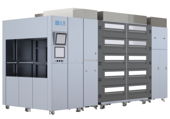
Coat Developer Equipment

12 & 8 inches or compatible

  • Applicable wafer size: 12 & 8 inches or compatible
  • Equipment dimensions: 5890(D) x 2425(W) x 3300(H) mm
  • Application fields: silicon-based semiconductors, compound semiconductors (GaAs, GaN, SiC, filters), MEMS, advanced packaging, and other fields.

Product advantages:

  1. Supports interfacing with Canon, Nikon, and ASML lithography machines
  2. Front-end supports KrF and ArF processes; back-end supports I-line and PI processes
  3. Five-layer stacked frame structure, small footprint
  4. Adopts a brand-new architecture, WPH > 250
  5. 20 spin units, 60 hot/cold plates
  6. Equipment configuration can be customized according to customer needs
  7. Supports TRMS and EAP automation systems
  8. Supports SECS communication and AMHS systems
  9. SVID output available, supports FDC
  10. Supports OHT overhead hoist transport

Independent research and development

  • Software Running
  • Mechanical Transmission
  • Circuit Module
  • Unit for Coating
化合物半导体

工艺能力:> 0.18um产品:砷化镓(GaAs) ,氮化镓(GaN),碳化硅(SiC), 滤波器 (Filter)

微机半导体

工艺能力:> 0.18um产品:MEMS

硅基半导体

工艺能力:> 90nm产品:IGBT ,CMOS ,MPU ,MCU,DSP,RAM,ROM,Flash ,